Micro
LED has become a high-profile advanced technology in the display industry, where related applications appear from time to time. For example, leading players, such as AUO, Innolux and PlayNitride, presented the results of Micro LED development by showcasing their innovations during the Touch Taiwan 2021 exhibition. These new products have altogether revealed display makers’ determination to overcome the existing technical problems of Micro LED production and ultimately realize mass production.
To achieve mass production with a lower cost and desirable yield rate, manufacturers must—in addition to mass transfer—improve inspection and repair technologies, which are indispensable for Micro LED production. However, identifying and repairing defective chips accurately and rapidly among countless tiny Micro LEDs remains a huge challenge.
To enhance Micro LED inspection efficiency, R&D personnel and equipment providers have continued to advance mass inspection technologies. UNX Technologies, for example, has developed the infrared (IR) radiation microscope EM series, a useful failure analysis tool with high positioning accuracy that can quickly identify defective Micro LEDs through thermal energy detection.
Using Heat-based Approach to Finding Defects, UNX Produces Inspection Equipment with High Efficiency
UNX chairperson Lai Yu-An said that producers mostly identify defective chips using thermocouples with increased operating voltage orcurrent, yet this approach can easily cause damage and distortion. To solve the problem, UNX turned to adopt a non-destructive, non-contact solution, namely the “thermal energy” inspection. Because a defective component tends to differ from its normal counterparts once being energized, manufacturers often detect it through energy (light and heat) measurements.
(Lai Yu-An, chairperson of UNX Technologies; image source: UNX)
As Lai specified, there are three common energy measurements, namely the photo emission measurement, OBIRCH and thermal emission measurement. UNX adopts the third approach.
When an object’s temperature is higher than absolute zero, it emits radiation. Therefore, we can use thermal imaging systems (or IR cameras) to confirm whether electronic components (e.g., ICs and displays) have a “fever”—just like we do for human beings.
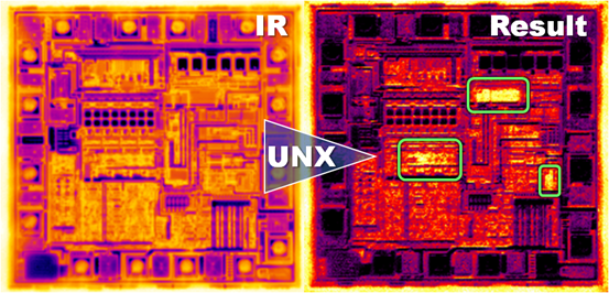
(IC inspection; image source: UNX)
As manufacturing processes advance with smaller product size and lower operating voltage, the resultant heat changes accordingly; consequently, to accurately identify defect-generated heat becomes more difficult. Therefore, an IR radiation microscope featuring high magnification is required. For example, UNX’s EM series integrate a high-magnification IR cameras and signal analysis, which can locate where exactly the defect is.
Lai continued to emphasize that an advantage of IR measurement lies on its non-contact nature, which does not affect thermal performance and results of high-frequency measurement. By cooperating with HOPE Visionlink Technology, UNX is able to adopt InfraTec’s made-in-Germany IR cameras featuring various magnifications for different product size specs, thereby enabling the implementation of desirable measurements. Some of these InfraTec cameras can capture 1,000 frames per second (high sampling rate) and even achieve a rate of 30,000 fps in the sub-frame mode. With such cameras, the IR system can record the temperature in every moment, facilitating signal processing and analysis.
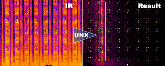
(Low-magnification IR image of Mini LEDs; source: UNX)
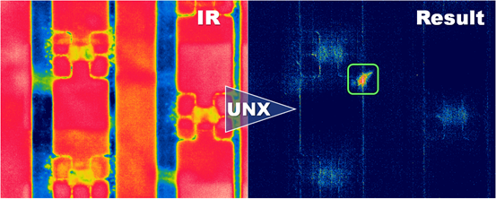
(High-magnification IR image of Mini LEDs; source: UNX)
Along with UNX’s scanning technology, the IR cameras can obtain ultra-wide field of view and take detailed wide-angle pictures suitable for large-scale display measurement. With appropriate settings, the cameras automatically move and measure IR energy; the obtained images are then combined into a large thermogram with maximum resolution of 9600×7680 pixel. Additionally, UNX can provide high-quality pictures using pixel shifting, with the resolution being 6400×5120 pixel at maximum.
In addition to automatic measurement, UNX’s EM series are equipped with signal processing, which can reduce noise, locate defects and make image analysis straightforward.
The thermal IR inspection results are often analyzed manually by experienced engineers, which requires long-term training for effective defect identification. Moreover, IR radiation lens—regardless of the level—can only detect the surface temperature and cannot penetrate any objects, making analysis fully dependent on the obtained measurements. Manual analysis has also become difficult as manufacturing processes are increasingly complex, which is why UNX chose to integrate signal processing with its EM products.
Signal processing, as Lai explained, is similar to noise reduction during data transmission, only it is used in IR spectroscopy that is easily affected by the surroundings and material properties. Signal processing makes visualization of measurement results easier with precise coordinate-based analysis and location. Only with such technology can the varying conditions between the superficial–deep layers of an object be presented. In addition to display measurement, signal processing can be applied to IC failure analysis (e.g., for determining short circuits and leakage).
“We offer a simple, easy-to-use device enabling standardized measurement without strict requirements. With this tool that helps interpret measurement results, even a rookie can successfully conduct a thermal IR test,” concluded Mr. Lai.
Highly Integrated EM Products Reduce Difficulty in Micro LED Inspection
(IR radiation microscope: the EM series; image source: UNX)
To sum up, simply determining temperature distribution for defect detection might no longer work as products are becoming increasingly small, while previous inspection models cannot accurately identify defect-produced heat. Therefore, UNX developed a series of IR radiation microscopes (i.e., the EM products)—in which signal processing is incorporated with high-sensitivity cameras and an axis control system—featuring auto focus and image cropping as well as straightforward operation. Because the high-sensitivity cameras can directly identify problematic components with no need to increase voltage/current (which might damage components), the EM products can discover defects under normal or low workload.


