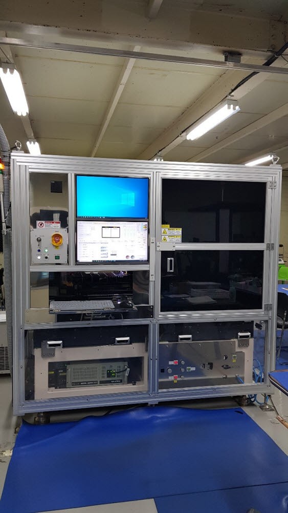
Realization of side wiring with 10㎛ ultra-fine laser
Solved problems of separation process of the glass substrate.
Shorten 3D pattern printing process to 50 to 5 minutes

A small and medium-sized company has developed a core process technology for the next-generation microLED display that will succeed the organic light emitting diode (OLED). It is an ultra-fine laser technology necessary to implement wiring on the side of a thin glass substrate, and is expected to increase the yield of micro LEDs and speed up commercialization.
Laser apps (CEO Eun-sook Jeon) announced that it has secured laser technology to implement side wiring of microLED displays after four years of research and development on the 17th.
MicroLED is considered a next-generation technology that will compensate for OLED shortcomings as it can use LED devices instead of organic materials and implement super-large displays through tile-type assembling methods.
However, there is a risk of separation when attaching thin glass substrates like tiles, and there are disadvantages as it is difficult to implement wiring on the substrate. Laser apps has dramatically improved the microLED process problems with its own proprietary laser technology.
Laser apps technology minimizes thermal effects and does not generate microcracks when cutting TFT glass substrates. Existing technologies are at risk of damaging glass substrate wiring and coating due to heat generated during cutting, which has been removed. Since microcracks do not occur, post-processing processes such as grinding are not required.
It solved the problem of separation that may occur when the substrate is connected by precisely cutting the glass substrate with a deviation within 10 micrometers (μm). MicroLEDs can freely adjust the display size by attaching several small substrates. If the screen is broken, only the substrate needs to be replaced.
It also secures a technology that accurately produces 3D patterns on the side of glass substrates, which greatly helps in the difficulty of microLED wiring. In order to print 3D patterns on the side of a glass substrate with general laser technology, laser beams must be irradiated three times as top, bottom, and side, but laser apps were implemented at once. This process time has been reduced from 50 minutes to 5 minutes. The technology patent required for this process has been secured and the equipment has been developed. A line width of 10 μm is possible. Laser apps technology can be used for both glass substrates (rigid) and Ultra Thin glass (UTG) substrates.
Laser apps (CEO Eun-sook Jeon) said, "It is a technology that can be used not only in displays but also in industries including semiconductors," adding, "Only when securing the original technology for micro processing can beat China's pursuit and maintain the super gap."
By Staff Reporter Yong-joo kim (kyj@etnews.com)
2022 Global LED Video Wall Market Outlook and Price Cost Analysis
Release Date: September 2021
Language: Traditional Chinese / English
Format: PDF
|
If you would like to know more details , please contact:
|


