 2012-09-07
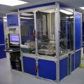
Kyma Technologies has tapped into the market for GaN crystal growth equipment. The firm’s GaN crystal growth system is based on the hydride vapour phase epitaxy (HVPE) growth process which is a proven high growth rate approach for producing high purity crystalline compound semiconductor materials including GaN, GaAs, InP, and CdS. HVPE is the dominant process used today for production of free-standing GaN substrates and recently has been used by Kyma and others to produce high quality GaN on sapphire templates and GaN on silicon templates. HVPE g...
Continue reading →
 2012-05-24
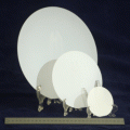
Kyma Technologies Inc of Raleigh, NC, USA, has made a breakthrough on a 10-inch diameter AlN-on-sapphire template using its patented plasma vapor deposition of nanocolumns (PVDNC) technology. The PVDNC AlN templates are chosen by manufacturers of blue, green and white LEDs as a replacement for bare and patterned sapphire substrates. The 250mm (10-inch) sapphire substrate was provided by Monocrystal Inc of Stavropol, Russia, which provides sapphire products and metallization pastes to the semiconductor, optical, and photovoltaic industries. According ...
Continue reading →
2011-08-05
Kyma’s new n+ GaN substrate product line will boast a bulk resistivity specification of < 0.02 Ω -cm, which is two orders of magnitude lower in resistivity than Kyma’s previously offered n-type GaN.
What’s more, Kyma has successfully produced n+ bulk GaN wafers with measured carrier concentrations of up to 6 x 1018cm-3and corresponding bulk resistivities of < 0.005 Ω –cm. The firm’s n-type GaN product is still being offered and, for distinction, is being relabelled as n- GaN (“nminus” GaN). I...
Continue reading →
2010-09-10
Sensor Electronic Technology (SETI) has signed a Joint Development Agreement with Kyma Technologies, of Raleigh, NC, USA, aiming at developing low defect AlGaN substrates and high performance optoelectronic and electronic devices.
It's reported that SETI will center its device development efforts on next generation high efficiency Deep UV LEDs on these novel substrates as it grows its markets in high power applications such as water disinfection.
Continue reading →
2010-02-05
Kyma Technologies, Inc., a leading supplier of ultra-high purity crystalline gallium nitride (GaN) and aluminum nitride (AlN) materials and related products and services, is slated to receive $2.8 million from the U.S. Department of Defense (DOD) for the continued development of low defect density GaN materials for high performance electronic device applications.
Continue reading →
 2012-09-07
 2012-05-24


