 2016-04-14
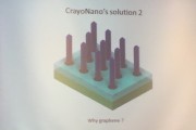
The LED industry is hunting for innovative technologies and application fields, as lighting and backlight market growth wane. UV LEDs over the past year has caught many LED manufacturers attention, the budding UV-A LED market application sector in nail curing, air purification, and printing applications is attracting top LED players including Nichia and Osram to invest in the sector. UV-C LED or DUV LED that has a wavelength ranging from 200 nm to 280 nm remains a market sector that barely exists at the moment, due to certain technical challenges that call for new solutions.
Continue reading →
 2016-04-12
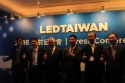
LED Taiwan to take place in Hall 1 of Nangang Exhibition Center starting this Wednesday has added three new theme pavilions including LED Components, Power Device Pavilion, Smart Lighting Pavilions, said organizers during a press conference held at Taipei World Trade Center Club, Taiwan earlier this afternoon.
Continue reading →
2013-09-04
LED Taiwan’s 2013 Semiconductor Equipment and Materials International (SEMI) exhibition will be launched on Sept. 4, 2013 to present the latest technology from domestic and international LED manufacturers and suppliers. Main themes of forums hosted at the show will include “LED technology forum,” “2013 Automation Technology for Solid-State Lighting Workshop,” and “TechXPOT”. Over the last year, the LED industry has been more cautious in expansions, and has been elevating its oversupply situation.
Continue reading →
2013-01-11
SEMI's HB-LED Standards Committee has approved its first standard, specifying sapphire wafers used in making HB-LED devices. Five categories of single-crystal, single-side polished c-axis sapphire wafers are covered by the new HB1 standard: • Flatted 100mm diameter, 650μm thick, • Flatted 150mm diameter, 1,000μm thick, • Flatted 150mm diameter, 1,300μm thick, • Notched 150mm diameter, 1,000μm thick, and • Notched 150mm diameter, 1,...
Continue reading →
2011-04-28
Recently, SEMI has developed an agreement with Korea Polytechnic University(KPU) on a talent training program for the LED and photovoltaic industries.
Under the MOU, the first LED manufacturing training program will be held at the COEX in Seoul from October 24-26, 2011. The two organizations will join force to develop the curriculum that offers both theoretical and practical training. In particular, KPU offers LED facilities and equipment to supply gain hands-on experience in the LED manufacturing process technology.
SEMI is involved in several...
Continue reading →
2011-01-20
SEMI and Yole Développement are partnering on a webinar series on HB-LED manufacturing on February 9, March 2, and March 23. See below for more information on these valuable opportunities to expand your business in the long term, transformational trend to solid state lighting and other HB-LED applications. The SEMI—Yole Développement 3-part webinar series on HB-LED manufacturing will take place on February 9, March 2, and March 23 at 10:00am Pacific (1:00pm Eastern). This seminar series will be among the most comprehensive overview...
Continue reading →
2010-12-09
SEMI noted that fab spending would increase about 18.3% in 2011 and about 9.5% in 2012, with the ongoing technology upgrades and continued capacity growth, especially in LED segment.
In 2011, the spending on construction projects would decrease about 11% and in 2012 it would become much less due to a currently uncertain outlook for new fab construction starts. But it estimated that spending on fab equipment would rise 23% to about US$40 billion in 2011.
Continue reading →
2010-11-22
SEMI has set up a HB-LED standards committee, which initiated standards task forces on four critical areas of LED manufacturing: wafers, carriers, assembly and automation.
According to SEMI, ''Unlike silicon wafers used in semiconductor manufacturing, there currently are no industry standards addressing wafer geometries, surface characteristics, wafer ID, wafer orientation, and other features, resulting in costly proliferation of wafer types and styles. ''
Continue reading →
 2016-04-14
 2016-04-12


