University of California Santa Barbara (UCSB) in the USA suggests that indium gallium nitride (InGaN) red micro-sized light-emitting diodes (μLEDs) could provide a solution for displays [Panpan Li et al, Appl. Phys. Lett., v119, p081102, 2021].
Although the high indium content leads to relatively low external quantum efficiency (EQE) compared with commercial aluminium indium gallium phosphide (AlInGaP) regular-size LEDs, which can reach 20-30%, the UCSB research shows that the InGaN devices maintain their ~2.5% EQE as the dimensions scale down to the tens of microns level.
By contrast, AlInGaP μLEDs suffer from severe degradation of the EQE as the size decreases. This suggests a sidewall surface effect, since the mesa perimeter becomes increasingly important relative to the bulk in smaller devices.
μ
LED-based displays should enable higher resolution, high contrast ratio, longer lifetime, and lower power consumption in comparison with traditional technologies such as liquid-crystal displays (LCDs). Other potentials include wearable devices, ultra-large and very small display screens, augmented reality (AR), virtual reality (VR), and visible light communication.
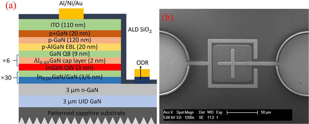
The UCSB μLED material (Figure 1) was grown on patterned sapphire using atmospheric-pressure metal-organic chemical vapor deposition (MOCVD). The 3μm GaN buffer was unintentionally doped (UID).
Figure 1: (a) Schematic epitaxial structure of InGaN red μLEDs; (b) Scanning electron micrograph of fabricated 60μmx60μm μLED.
The light-emitting multiple quantum well structure consisted of six periods of red-emitting indium gallium nitride (InGaN), an aluminium gallium nitride (AlGaN) cap, and GaN quantum barrier. For red light with wavelengths longer than 600nm, the indium content should be more than 35%.
The purpose of the AlGaN cap was to increase the peak EQE. Previous research suggests that the cap could prevent desorption of indium from the well during growth, and partially compensate for the compressive strain of InGaN relative to the GaN lattice.
The fabricated square μLEDs ranged from sides measuring 100μm down to 20μm. Transparent indium tin oxide (ITO) was used as the top p-contact. The devices included an omni-directional reflector (ODR) layer constructed from silicon dioxide and tantalum pentoxide layers. Atomic layer deposited (ALD) SiO2 was also used to passivate the mesa sidewalls of the μLED, to reduce surface recombination from the reactive ion etch damage. The contact electrodes consisted of aluminium/nickel/gold (Al/Ni/Au).
The forward voltage for 20A/cm2 current density was 3.7V for devices with sides from 40μm to 100μm. The smallest 20μm device had an even lower forward voltage of 3.5V, which the team suggests resulted from more effective current spreading in the ITO of the smaller device.
The light output power (LOP) increased approximately linearly with current injection, with the curves from the different size devices overlapping over their respective current domains. The LOP for the 100μm device reached 0.83mW at 20mA.
The spectrum of the red light peaked at 611nm with 48nm full-width at half-maximum (FWHM) at 3A/cm2. The researchers report that there was no short-wavelength peak from the 30-period InGaN/GaN superlattice on the n-GaN layer, suggesting electron-hole injection was restricted to the red-emitting quantum wells.
At higher injection the peak blue-shifted to 588nm at 200A/cm2. The shift was attributed to higher localized states filling up at higher current, increasing the effective bandgap, along with screening of the charge-polarization electric fields of the epitaxial structures. This large blue-shift would not be welcome in color display applications.
The peak EQE for 80μm and 100μm LEDs was around 2.6%, with the peak coming for injection in the range 10-20A/cm2. The 20μm device had a slightly reduced value of 2.4%. The EQE range at 100A/cm2 was 2.3-2.5% for the 20μm to 100μm devices.
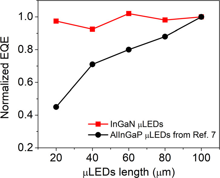
The researchers also compared the size dependence of the peak EQE with that of aluminium indium gallium phosphide (AlGaInP) devices produced by UCSB and Seoul Viosys Co Ltd of South Korea (Figure 2). The AlGaInP structure showed a 57% reduction in EQE in going from sides of 100μm down to 20μm, while the InGaN μLEDs showed relatively stable performance.
Figure 2: Comparison of normalized peak EQE for square InGaN and AlInGaP red μLEDs with different side lengths.
The researchers comment on the AlGaInP μLED EQE: “This is caused by the SRH [Shockley-Read-Hall] carrier injection loss due to a higher surface recombination velocity of AlInGaP, which is related to the fundamental property of the materials and difficult to overcome.” The SRH mechanism is the major non-radiative recombination route at low current density.
The team also points out that μLED display proposals suggest the need for 5μmx5μm red-emitters with 5% EQE, adding “we believe that InGaN red μLEDs would have large potentials for such efficiencies.”


